10 things to consider when planning your PCB Layout

Before we provide a quote to any potential customers, we review their Gerber files to help us get an understanding of exactly what it is we are dealing with. Aside from evaluating the Gerber file for printing, when we review a Gerber file, our technicians will look for two things on a PCB layout:
- Opportunities for our clients to save money on PCB production without compromising on the quality and performance.
- Potential risk areas where, due to design, the board will be prone to shorts and opens.
Here are ten tips to help you keep cost down when looking at your PCB layout and minimise risk areas when designing your Printed Circuit Board.
1. Technology’s great, but run a manual check too.
Before sending your Gerber files to be produced, print a checklist of all the connections needed for your PCB layout to work, and manually cross off each one as you check that it’s been incorporated into the design.
2. Create a useful Silk Screen layer.
Use the Silk Screen layer to identify any board details, LEDs or connecters. Consider adding your order number or a batch number too.
3. Do you really need a 4 layer board, or will a 2 layer board suffice?
You could make substantial cost savings if you can get away with using a 2 layer board in place of a 4 layer board.
4. Plan trace thickness.
Use a trace width calculator to work out how thick and wide your traces need to be to deliver the performance you need, accounting for the voltage drop, power dissipation and increase in temperature that will take place once current starts to flow through the copper.
5. Consider cooling time within your layers.
When designing your PCB remember that traces in internal layers cool slower than those in external layers because heat has to travel through the external layers to dissipate.
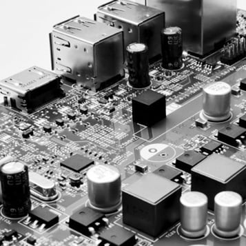
6. Component placement
Carefully consider the placement of components on your PCB layout to optimise performance and reduce signal interference. Group related components together and place them strategically to reduce trace lengths and redirect signal paths. Pay attention to high-speed signal traces and sensitive components, ensuring adequate separation and proper grounding to minimise noise and signal degradation.
7. Design for manufacturability (DFM)
Keep manufacturability in mind throughout the PCB layout process to streamline production and reduce costs. Avoid complex shapes or overly dense component placement that may increase manufacturing difficulty and lead to higher production costs. Optimise your design for automated assembly processes and ensure compatibility with standard PCB manufacturing techniques to simplify production and minimise errors.
8. Signal integrity
Pay close attention to signal integrity considerations when planning your PCB layout to ensure the reliable operation of your electronic circuits. Minimise signal distortion, reflections, and crosstalk by carefully routing high-speed signal traces and maintaining consistent impedance throughout the board. Use techniques such as controlled impedance routing, differential signalling, and proper termination to preserve signal integrity and lower signal degradation.
9. Power distribution
Plan your power distribution network carefully to commit stable and efficient power delivery to all components on the PCB. Design a robust power distribution system with adequate power planes, bypass capacitors, and voltage regulators to minimise voltage fluctuations, noise, and electromagnetic interference (EMI). Consider the current requirements of each component and optimise power trace widths and placement to reduce voltage drops and power losses.
10.Testing and debugging
Incorporate test points, features, and diagnostic indicators into your PCB layout to facilitate testing and debugging during manufacturing and assembly. Include access points for probe connections, test pads for measuring critical signals, and LED indicators for visual feedback on board status. Design your PCB layout with ease of testing and troubleshooting to expedite the debugging process and ensure faster time to market for your electronic products.
Conclusion:
Designing a practical PCB layout requires careful consideration of multiple factors to ensure optimal performance, reliability, and cost-effectiveness. By following these 10 tips, you can streamline the PCB layout process, minimise production costs, and reduce the risk of design errors and manufacturing issues. Remember to collaborate closely with your PCB manufacturer and utilise their expertise to optimise your design for manufacturability and reliability. Ready to start planning your PCB layout? We are just one message away to discuss your project requirements and develop a strategy to help you achieve your goals with high-quality, cost-effective PCB solutions.